Neural Interfacing ICs
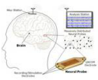
The research of Biomedical Interfaces is all about innovation of new human machine interfaces through skin, heart, central and peripheral nervous system. Our neural interfacing circuit research is devoted to innovation of state of the art brain-machine interfaces, high density neural recording, and stimulation microsystems.
|
A Battery-Powered Opto-Electrophysiology Neural Interface with Artifact-Preventing Optical Pulse Shaping
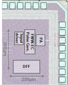
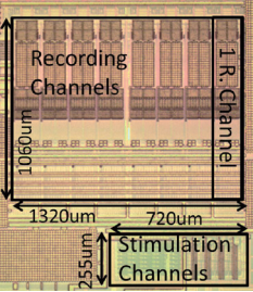
We present a neural interface IC for high-precision optical stimulation and electrical recording from implanted optoelectrodes with the highest system integration to date. The system combines 12 high-resolution constant-current LED driver channels, 32 recording channels, and an efficient PMU for operation from a low voltage Li battery on a wireless platform. A novel LED driver architecture features a high-efficiency wide-current-range fully-integrated voltage regulator and a high-resolution pulse shaper to minimize recording artifacts from sharp current pulse edges. A prototype, fabricated in 0.18μm CMOS, occupies 7.35mm². The LED driver has a peak efficiency of 50% and consumes 31μW quiescent power. We demonstrate in-vivo that the pulse-shaping scheme prevents stimulation artifacts. [A. E. Mendrela, S.-Y. Park, M. Vöröslakos, M. P. Flynn, and E. Yoon, "A Battery-Powered Opto-Electrophysiology Neural Interface with Artifact-Preventing Optical Pulse Shaping," IEEE Symposium on VLSI Circuits, Jun. 2018.] |
|
High-Resolution Opto-Electrophysiology System with a Miniature Integrated Headstage
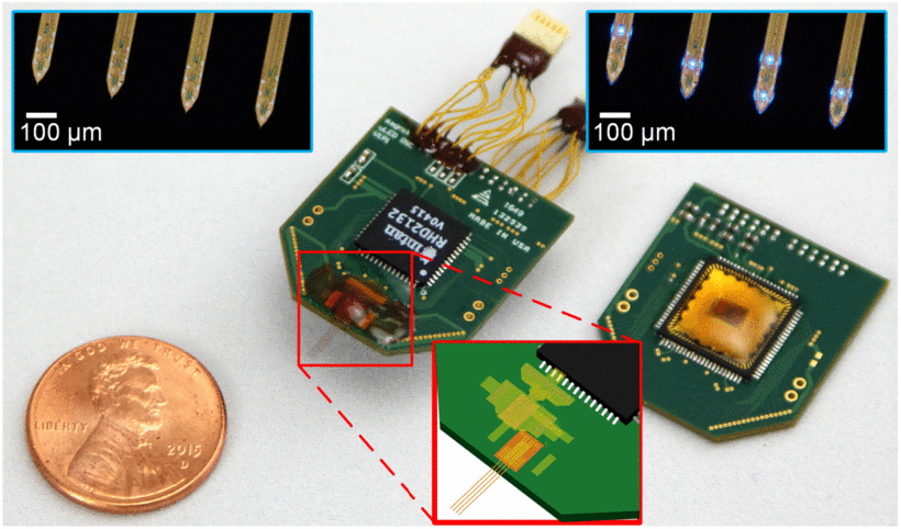
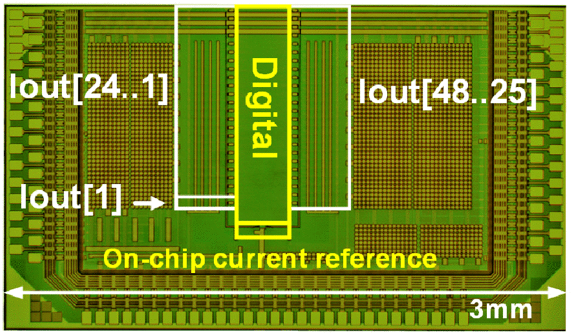
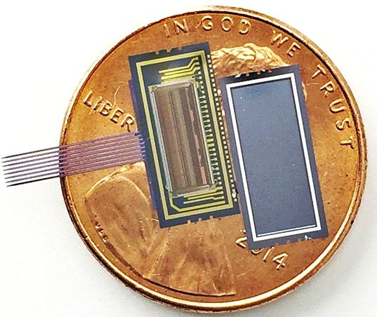
This work presents a fully integrated neural interface system in a small form factor (1.9 g), consisting of a μLED silicon optoelectrode (12 μLEDs and 32 recording sites in a 4-shank configuration), an Intan 32-channel recording chip, and a custom optical stimulation chip for controlling 12 μLEDs. High-resolution optical stimulation with approximately 68.5 nW radiant flux resolution is achieved by a custom LED driver ASIC, which enables individual control of up to 48 channels with a current precision of 1 μA, a maximum current of 1.024 mA, and an update rate of >10 kHz. Recording is performed by an off-the-shelf 32-channel digitizing front-end ASIC from Intan. Two compact custom interface printed circuit boards were designed to link the headstage with a PC. The prototype system demonstrates precise current generation, sufficient optical radiant flux generation (Φe > 0.16 μW), and fast turn-ON of μLEDs (trise < 10 μs). Single animal in vivo experiments validated the headstage's capability to precisely modulate single neuronal activity and independently modulate activities of separate neuronal populations near neighboring optoelectrode shanks. [A. E. Mendrela, K. Kim, D. English, S. McKenzie, J. P. Seymour, G. Buzsáki, and E. Yoon, "A High-Resolution Opto-Electrophysiology System with a Miniature Integrated Headstage," IEEE Transactions on Biomedical Circuits and Systems, vol. 12, no. 5, pp. 1065-1075, Oct. 2018.] |
|
4.32 pJ/b, Overlap-Free, Feedforward Edge Combiner-Based Ultra-Wideband Transmitter for High Channel-Count Neural Recording
We present an ultralow-power, ultra-wideband (UWB) transmitter (TX) in standard 65-nm CMOS processes. The TX consists of feedforward edge combiners and interpolators for ultralow-power operation and reliable pulse generation that is essential in UWB TXs. The implemented circuit avoids pulse overlapping without complicated calibrations and has achieved an energy efficiency of 4.32 pJ/b at 200-Mbps data rate. The TX is suitable for energy-constraint, high-data-rate applications such as wireless telemetry in implantable high-density neural recording interfaces [Y.-J. Lin, S.-Y. Park, X. Chen, D. Wentzloff and E. Yoon, "4.32-pJ/b, Overlap-Free, Feedforward Edge-Combiner-Based Ultra-Wideband Transmitter for High-Channel-Count Neural Recording," IEEE Microwave and Wireless Components Letters, vol. 28, no. 1, pp. 52-54, Jan. 2018.] |
|
Dynamic Power Reduction in Scalable Neural Recording Interface Using Spatiotemporal Correlation and Temporal Sparisty of Neural Signals
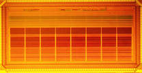
We report a scalable neural recording interface with embedded lossless compression to reduce dynamic power consumption for data transmission in high-density neural recording systems. The prototype chip was fabricated using 180 nm CMOS processes, incorporating 128 channels in a modular architecture that is easily scalable and expandable for high-density neural recordings. The fabricated chip achieved the data rate reduction for the LFPs and spikes by a factor of 5.35 and 10.54, respectively, from the proposed compression scheme. Consequently, PD was reduced by 89%, when compared to the uncompressed case. We also achieved the state-of-the-art recording performance of 3.37 µW per channel, 5.18 µVrms noise, and 3.41 NEF2VDD. [S.-Y. Park, J. Cho, K. Lee, E. Yoon, "Dynamic Power Reduction in Scalable Neural Recording Interface Using Spatiotemporal Correlation and Temporal Sparsity of Neural Signals," IEEE J. Solid-State Circuits, vol. 56 no. 4, pp. 1102-1114, Apr. 2018 (invited)] |
|
Modular 128-Channel Δ-Δ Σ Analog Front-End Architecture Using Spectrum Equalization Scheme for 1024-Channel 3-D Neural Recording Microsystems
We report an area- and energy-efficient integrated circuit architecture of a 128-channel Δ-modulated Δ Σ analog front-end (Δ-Δ Σ AFE) for 1024-channel 3-D massive-parallel neural recording microsystems. In order to reduce both area and energy consumption in the recording circuits, we implemented a spectrum equalization scheme to take advantage of the inherent spectral characteristics of neural signals, where most of the energy is confined in low frequencies and follows a ~1/f curve in the spectrum. This allows us to implement the AFE with a relaxed dynamic range by ~30 dB, thereby contributing to the significant reduction of both energy and area without sacrificing signal integrity. The single-channel AFE consumes 3.05 μW from 0.5 and 1.0 V supplies in an area of 0.05 mm² with 63.8-dB signal-to-noise-and-distortion ratio, 3.02 noise efficiency factor (NEF), and 4.56 NEF²VDD. [S.-Y. Park, J. Cho, J. K. Na, E. Yoon, "Modular 128-Channel Δ-Δ Σ Analog Frontend Architecture Using Spectrum Equalization Scheme for 1,204-Channel 3-D Neural Recording Microsystems," IEEE J. Solid-State Circuits, vol. 53, no.2, pp. 501-514, Feb. 2018.] |
|
Bidirectional Neural Interface Circuit With Active Stimulation Artifact Cancellation and Cross-Channel Common-Mode Noise Suppression
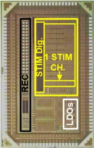
This work presents a bidirectional neural interface circuit that enables simultaneous recording and stimulation with a stimulation artifact cancellation circuit. The system employs a common average referencing (CAR) front-end circuit to suppress cross-channel environmental noise to further facilitate use in clinical environment. This paper also introduces a new range-adapting (RA) SAR ADC to lower the system power consumption. A prototype is fabricated in 0.18 μm CMOS and characterized and tested in vivo in an epileptic rat model. The prototype attenuates stimulation artifacts by up to 42 dB and suppresses cross-channel noise by up to 39.8 dB. The measured power consumption per channel is 330 nW, while the area per channel is 0.17 mm². [A. E. Mendrela, J. Cho, J. A. Fredenburg, V. Nagaraj, T. I. Netoff, M. P. Flynn, E. Yoon, "A Bi-Directional Neural Interface Circuit with Active Stimulation Artifact Cancellation and Cross-Channel Common-Mode Noise Suppression," IEEE J. Solid-State Circuits, vol. 51, no. 4, Apr. 2016] |
|
Efficient Power Management Integrated Circuit for Implantable Biomedical Systems
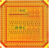
We report a pulse width modulation (PWM) buck converter achieving high power conversion efficiency (PCE) at ultra-light loads (<100µA) for implantable biomedical systems. In order to achieve high PCE while operating in 1MHz, fixed frequency, the buck converter actively reconfigures the size of the power PMOS, NMOS transistors, and their gate drivers in accordance with the load currents. The buck converter adopts the hybrid (digital/analog, i.e., coarse/fine) control mode to realize the reconfigurable power trains with minimum power consumption. The buck converter achieved 86.3% peak efficiency at 1.4mA, over 80% efficiency from 45µA to 4.1mA load conditions generating 1V output from 2.5-3.3V single supply. [S.-Y. Park, J. Cho, K. Lee, and E. Yoon, “PWM Buck Converter with >80% PCE in 45μA-to-4mA Loads Using Analog-Digital Hybrid Control for Implantable Biomedical Systems,” IEEE ISSCC (International Solid-State Circuit Conference) Technical Digest, pp. 303-305, Feb. 2015] |
|
Analog Front-End Module With Moderate Inversion and Power-Scalable Sampling Operation for 3-D Neural Microsystems
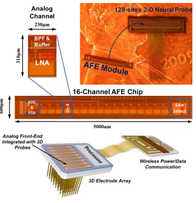
We report an analog front-end prototype designed in 0.25 CMOS process for hybrid integration into 3-D neural recording microsystems. For scaling towards massive parallel neural recording, the prototype has investigated some critical circuit challenges in power, area, interface, and modularity. We achieved extremely low power consumption of 4 uW/channel, optimized energy efficiency using moderate inversion in low-noise amplifiers (K of 5.98 or NEF of 2.9), and minimized asynchronous interface (only 2 per 16 channels) for command and data capturing. We also implemented adaptable operations including programmable-gain amplification, power-scalable sampling (up to 50 kS/s/channel), wide configuration range (9-bit) for programmable gain and bandwidth, and 5-bit site selection capability (selecting 16 out of 128 sites). The implemented front-end module has achieved a reduction in noise-energy-area product by a factor of 5–25 times as compared to the state-of-the-art analog front-end approaches reported to date. [Al-Ashmouny, K.M.; Sun-Il Chang; Euisik Yoon, "A 4 Analog Front-End Module With Moderate Inversion and Power-Scalable Sampling Operation for 3-D Neural Microsystems," IEEE Transactions on Biomedical Circuits and Systems , vol.6, no.5, pp.403,413, Oct. 2012] |
|
BioBolt: A Minimally-Invasive Neural Interface for Wireless Epidural Record by Intra-Skin Communication
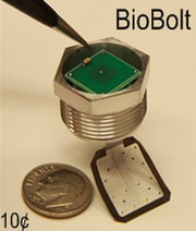
Recent technology progresses in CMOS and MEMS technologies have enhanced monitoring capability of neural activities for diagnosis of neural disorders, brain-machine interface and prosthetic applications. Recently, epidural recording gains its attention as an optimal solution for balanced signal fidelity and safety. In this paper, we report a bolt-shape Minimally-Invasive Neural Interface, BioBolt, which have (1) Low-Power Analog Front-Ends, (2) Epidural Record Capability in order to minimize any infection and tissue reaction, and (3) Intra-Skin Communication for low-power data transmission. [Sun-Il Chang, Khaled Al-shmouny, Mike McCormick, Yu-Chih Chen and Euisik Yoon, “BioBolt: A Minimally-Invasive Neural Interface for Wireless Epidural Recording by Intra-Skin Communication,” IEEE Symposium on VLSI Circuits, pp. 146-147, Kyoto, Japan, June 2011] |
|
Low-Power Area-Efficient SAR ADC
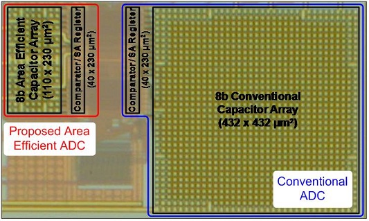
We report an area-efficient 8bit SAR ADC using dual capacitor array banks for brain signal interface microsystems. The proposed ADC consumes 680nW and the total chip area is 0.035 mm^2. We reduced the area and power by a factor of eight when compared with conventional approaches. If we increase the resolution, the area and power reduction factor exponentially increases in our architecture (e.g., a factor of 16 for 10 bit resolution). The measured SNDR, SFDR, THD, and ENOB are 42.82 +/- 0.47 dB, 57.90 +/- 2.82dB, -53.58 +/- 2.15 dB, and 6.65 +/- 0.07 bits, respectively. [Sun-Il Chang; Euisik Yoon, "A low-power area-efficient 8 bit SAR ADC using dual capacitor arrays for neural microsystems," Annual International Conference of the IEEE Engineering in Medicine and Biology Society, 2009 (EMBC 2009), pp.1647,1650, 3-6 Sept. 2009] |
|
Low-Power Low-Noise Pseudo-Open-Loop Preamplifier
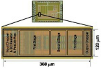
We report an energy efficient pseudo open-loop amplifier with programmable band-pass filter developed for neural interface systems. The proposed amplifier consumes 400nA at 2.5V power supply. The measured thermal noise level is 85nV/sqrt(Hz) and input-referred noise is 1.69uVrms from 0.3Hz to 1 kHz. The amplifier has a noise efficiency factor of 2.43, the lowest in the differential topologies reported up to date to our knowledge. By programming the switched-capacitor frequency and bias current, we could control the bandwidth of the preamplifier from 138 mHz to 2.2 kHz to meet various application requirements. The entire preamplifier including band-pass filters has been realized in a small area of 0.043mm2 using a 0.25um CMOS technology. [Sun-Il Chang; Euisik Yoon, "A 1μW 85nV/√Hz pseudo open-loop preamplifier with programmable band-pass filter for neural interface system," Annual International Conference of the IEEE Engineering in Medicine and Biology Society (EMBC 2009), pp.1631,1634, 3-6 Sept. 2009.] |
|
IBCOM: Intra-Brain Communication for Implantable Devices
We explore a new method of signal transmission for bio-implantable microsystems. Intra-brain communication or IBCOM is a wireless signal transmission method that uses the brain itself as a conductive medium to transmit the data and commands between neural implants and data processing systems outside the brain. Two miniaturized IBCOM (?IBCOM) CMOS chips were designed and fabricated for an in vivo test bed to transmit two prerecorded neural signals at different binary frequency shift keying (BFSK) carrier frequencies to validate the feasibility of IBCOM concept. The chips were packaged for full implantation in a rat brain except for external power delivery. The original neural signal waveforms were successfully recovered after being transmitted between two platinum electrodes separated by 15 mm with transmission power less than 650 pJ/bit for the CMOS implementation. [Al-Ashmouny, K.M.; Boldt, C.; Ferguson, J.E.; Erdman, A.G.; Redish, A.D.; Euisik Yoon, "IBCOM (intra-brain communication) microsystem: Wireless transmission of neural signals within the brain," Annual International Conference of the IEEE Engineering in Medicine and Biology Society (EMBC 2009), pp.2054,2057, 3-6 Sept. 2009] |

