CMOS Image Sensors
CMOS image sensors (CIS) provide miniaturized, low-power and low-cost solutions for a variety of imaging applications. Our research focuses on low-power imaging for wireless sensor node, optic flow sensor for micro-air vehicles, three-dimensional depth imaging, and optical cancer diagnosis.
|
CMOS Image Sensor with Simultaneous Energy Harvesting and Imaging Pixels
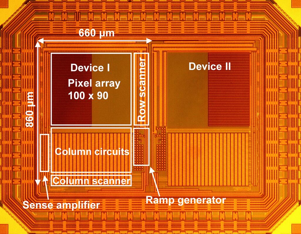
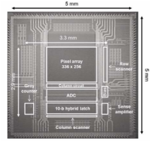
This prototype sensor demonstrates a CMOS active pixel that is capable of simultaneous imaging and energy harvesting without introducing additional in-plane p-n junctions. The prototype pixel uses a vertical p+/nwell/psub junction that is available in standard CMOS processes. Unlike the conventional CMOS electron-based imaging pixels, where the nwell region is used as a sensing node for image capture, we adopted a hole-based imaging technique, while exploiting the nwell region for energy harvesting at a high fill-factor of >94%. To verify the feasibility, CMOS image sensors are fabricated and characterized. We successfully demonstrated that the energy harvesting can be achieved with a power density of 998 pW/klux/mm2, while capturing images at 74.67 pJ/pixel. The fabricated prototype device has achieved the highest power density among the recent state-of-the-art works and can self-sustain its image capturing operation at 15 fps without external power sources above ∼60 klux of illumination. [S.-Y. Park, K. Lee, H. Song and E. Yoon, "CMOS Image Sensor Device for Simultaneous Imaging and Energy Harvesting," IEEE Electron Device Letters, vol. 39, no. 4, pp.532-535, Apr. 2018.] |
|
Time-of-Flight 3-D Camera with Adaptable Background Light Suppression Using Pixel-Binning and Super-Resolution
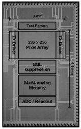
A 3-D camera which is insensitive to the background light (BGL) is implemented. Unlike most 3-D cameras, this sensor can operate in outdoors where the BGL can be higher than 100klx. This feature is implemented without increasing the pixel size, and hence achieving the smallest pixel size among all reported TOF sensors up to date. In addition, the sensor provides an adaptable BGL suppression using spatiotemporal resolution control by pixel-binning and super-resolution to guarantee the best image quality in all situations. [J. Cho, J. Choi, S.-J. Kim, J. Shin, S. Park, J.D.K. Kim and E. Yoon, "A 3-D Camera With Adaptable Background Light Suppression Using Pixel-Binning and Super-Resolution," JSSC, Aug., 2014] |
|
Integrated CMOS Optic Flow Sensor for Micro-Air-Vehicles
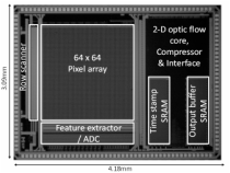
As a part of the Micro Autonomous Systems Technology (MAST) project, our partners and we are focusing on developing a bio-inspired micro air vehicle (MAV) whose autonomous navigation algorithm is borrowed from an insect’s visual system. Because of the simple nature of information processing in the insect’s visual system, which consists of multiple motion sensors to generate surrounding optic flows, this approach is one of the attractive candidates for low-power and low-payload autonomous navigation solutions. Our group is especially working on implementing a CMOS optic flow sensor to provide surrounding motion information that is accurate enough in order for the MAVs to autonomously and successfully control in both indoor and outdoor environments, while consuming extremely low power to satisfy severe MAV’s power budget. [S. Park, J. Cho, K. Lee and E. Yoon, “243.3pJ/pixel Bio-Inspired Time-Stamp-Based 2D Optic Flow Sensor for Artificial Compound Eyes,” IEEE International Solid-State Circuits Conference (ISSCC), 2014] |
|
Object-adaptive CMOS Image Sensor with Embedded Feature Extraction Algorithm
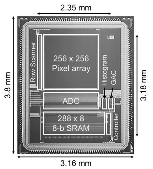
Distributed sensor nodes typically operate under the constraint of limited energy source, and power consumption is an important factor to extend the lifetime of sensor systems. Several low-power imagers have been reported for the application of wireless sensor network. However, the biggest power consumption comes from wireless signal transmission due to the large bandwidth of image signals. One way to reduce the bandwidth is to generate signals only when event happens by monitoring temporal changes. However, this event-based imaging has extraneous redundancy because the sensor may also respond to environmental conditions, such as change of illumination or background movement in addition to actual target objects. [J. Choi, S. Park, J.Cho, E. Yoon, "A 3.4 μW CMOS Image Sensor with Embedded Feature Extraction Algorithm for Motion-Triggered Object-of-Interest Imaging," Technical Digest of International Solid-State Circuits Conference, pp.478-479. Feb. 2013.] |
|
Energy/Illumination-adaptive CMOS Image Sensor with Reconfigurable Modes of Operations
For outdoor surveillance, sensitivity and dynamic range are important to deliver reliable images over widely changing illumination. However, constant monitoring with maximum awareness requires large power consumption and is not suitable for energy-limited applications such as battery-operated and/or energy-scavenging wireless sensor node. One of the ways to reduce power is voltage scaling. However, it significantly reduces the SNR and results in poor image quality. The signal can be easily corrupted from the noise in dark conditions or be saturated in bright conditions. Most imagers with high-sensitivity and wide dynamic range reported, consume large power > 50 mW, unsuitable for wireless imager node applications. Therefore, it is imperative to implement a sensor adaptable to environmental changes: e.g., the sensor keeps monitoring at extremely low power and only turns into high sensitivity or wide dynamic range operations when requested due to illumination changes or requested from the host for detailed image transmission. The sensor changes its operation back to the monitoring mode when enough operating energy is not available from the battery or energy-harvester. In this paper, we report an adaptive CMOS image sensor which employs four different modes: monitoring, normal, high-sensitivity and wide-dynamic-range (WDR) modes. This adaptable feature enables the reliable monitoring while significantly enhancing the battery lifetime for wireless image sensor nodes. A prototype chip has been fabricated using 0.18μm CIS process. We achieved a normalized power of 15.4 pW/frame•pixel (from the total power consumption) in monitoring mode. [J. Choi, S. Park, J.Cho, E. Yoon, “A 1.36uW Adaptive CMOS Image Sensor with Reconfigurable Modes of Operation from Available Energy/Illumination for Distributed Wireless Sensor Network,” Technical Digest of International Solid-State Circuits Conference, pp.112-114. Feb. 2012.] |
|
Multi-Resolution CMOS Image Sensor
A multi-resolution CMOS image sensor which simultaneously generates spatial-temporal multi-resolution images from dual channels: one for normal images ( 960 fps) with a reduced spatial resolution for moving objects in the region-of-interest (ROI). The entire image with the details in stationery objects and the suppressed motion-blur in moving objects can be acquired at low power consumption with optimal use of bandwidth. [J. Choi, S. -W. Han, S. -J. Kim, S. -I. Chang, and E. Yoon, ” A Spatial-Temporal Multiresolution CMOS Image Sensor With Adaptive Frame Rates for Tracking the Moving Objects in Region-of-Interest and Suppressing Motion Blur,” Journal of Solid-State Circuits, vol. 42, pp.2978-2989. 2007] |
|
Wide-Dynamic Range CMOS Image Sensor
A wide dynamic range CMOS image sensor with in-pixel floating-node analog memory for pixel level integration time control is implemented. There is no significant additional hardware in the pixel because we use a floating-node parasitic capacitor as an analog memory without additional timing budget. With the proposed sensor scheme, we could achieve the extended dynamic range by more than 42dB. [S. -W. Han, S. -J. Kim, J. Choi, C. -K. Kim, and E. Yoon, “A High Dynamic Range CMOS Image Sensor with In-Pixel Floating-Node Analog Memory for Pixel Level Integration Time Control,” Dig. Symp. VLSI Circuits, pp. 31-32, June 2006.] |
|
Low-Noise CMOS Image Sensor
A 512 x 384 CMOS image sensor in 0.18-um 1P4M technology with a 5.9 um pixel pitch to compensate for kTC reset noise, image lag, and fixed pattern noise has been implemented. A total of 330 uV(rms) random readout noise, which is a factor of two improvement over conventional reset operation, has been achieved. This can also suppress fixed pattern noise level to 250 uV(rms). |
|
CMOS Fingerprint Sensor with Integrated Column-Level Processor
A CMOS fingerprint recognition SoC with a new pixel architecture and embedded column-parallel processors optimized for 2-D digital image processing. The proposed sensor employs self-configuration column-parallel processors for adaptive filter operations and performs various image processing algorithms. The proposed pixel includes a sensing block, ADC and frame memory with no area penalty. [Kwang-Hyun Lee, Euisik Yoon, “A CMOS Image Sensor with Reset Level Control Using Dynamic Reset Current Source for Noise Suppression,” Technical Digest of International Solid-State Circuits Conference, pp.114-115. Feb. 2004.] |
|
CMOS Fingerprint Sensor with Pixel-Level Image Enhancement
A 500dpi capacitive-type CMOS fingerprint sensor includes pixel-level image enhancement. The parasitic capacitances between finger skin and a sensing electrode are rejected to enhance the sensitivity. During the readout, capacitive diffusion networks generate a locally-smoothed average signal that can be used as a local threshold level. This local threshold signal is subtracted from the original sensing signal using analog circuits within the pixel. The output image is centered on the local threshold level resulting in better quality for binarization process. [Kwang-Hyun Lee, Euisik Yoon, “A 500dpi Capacitive-Type CMOS Fingerprint Sensor with Pixel-Level Adaptive Image Enhancement Scheme,” Technical Digest of International Solid-State Circuits Conference, pp.282-283. Feb. 2002.] |
|
CMOS Image Sensor with Area-Efficient Correlated Double Sampling Scheme
Recently, CMOS image sensors (CIS) have been widely used because they have many advantages compared with CCD in terms of on-chip signal processing capability, low cost and low power consumption. However, the image quality of CIS is poor owing to high dark current, low sensitivity, and high readout noise. Among these, the readout noise problem has been a major issue in CIS. There have been many efforts to reduce readout noise using various correlated double sampling (CDS) circuits. The CDS circuit can effectively remove fixed pattern noise (FPN), which is the dominant noise source of CIS, and they are adopted in most commercial CIS products. However, as the number of pixels becomes larger and the size of pixel gets smaller in multi-mega pixel CISs, it is difficult to accommodate column-parallel CDS circuits in a small column pitch. [S.-W. Han and E. Yoon, “Area-efficient correlated double sampling scheme with single sampling capacitor for CMOS image sensors,” Electronic Letters, pp.335-336. Mar. 2006.] |
|
Megapixel CMOS Image Sensor
The size of pixel array in imaging device is getting larger. Beyond the digital still camera, image sensors are widely used in digital cinema and digital broadcasting system. Digital still camera above ten millions pixels is already commercialized. In digital broadcasting area, two megapixels HDTV is already into practical use, and eight megapixels HDTV is considered as next generation format. UDTV, which has nearly ten million pixels is under active technology development. As the number of pixels is increased, some undesirable effects like IR drop in power/ground line should be considered and more design efforts for speed and power consumption becomes required in design of CMOS image sensors. |

